
How not to design transmitters and receivers (part 7: phase comparators)
Wednesday 1 September, 2021, 08:31 - Amateur Radio, Broadcasting, Licensed, Pirate/Clandestine, Electronics
Posted by Administrator
One of the blocks yet to be discussed in the Wireless Waffle lockdown transmitter and receiver project is the phase/frequency comparator. In days of yore (a.k.a. the 1980s), the go-to integrated circuit (IC) for this function was the trusty 4046. This not only contains a couple of different types of phase comparator (the newest versions have three, the older ones just two) it also has a built in voltage controlled oscillator (VCO). The VCO works well up to a few MHz, or even higher depending on the specific type of IC, but is useless at VHF and thankfully can be easily inhibited. As, however, the phase comparator only needs to work at the reference frequency (usually a few kHz), the 4046 will function perfectly well in this role.Posted by Administrator
The 4046 takes the reference input on pin 14 (oddly termed the 'signal in' pin) and the variable frequency input on pin 3 (the 'comparator in'). The two phase comparator outputs are on pins 2 ('comparator I output') and 13 ('comparator II output'). On newer versions a third phase comparator output can be found on pin 15; on the older versions pin 15 has a Zener diode connected to it which is intended to be used to stabilise the power supply when using the VCO but was almost never employed.
;)
The Type I phase comparator is just an XOR gate. This produces a square wave output whose mark-space ratio varies with the difference in phase of the inputs. This can be fed into a loop filter to yield a voltage which varies up or down with the difference in phase. The primary difficulty with this method is that both the reference frequency, and the variable frequency input must be square waves with equal mark-space ratios. For the reference which is usually a square wave divided down from some crystal oscillator, this is usually not a problem, however the signal from the oscillator, following its traversal through the 'divide by N' circuit, is often just a pulse. Many divide by N devices just count a specific number of times, and when that count has been reached output a brief pulse. Additional circuitry is required to turn this into a square wave.
The Type II phase comparator is an altogether more sophisticated device and as well as not caring about the mark-space ratio of the two input signals, produces a positive 'up' or negative 'down' signal at its output instead of just a square wave. If its output is connected to a capacitor (through a suitable current limiting resistor) the voltage across the capacitor will only be given a push up or down if the phase of the input signals is different. If the two are fully in phase, the output of the Type II detector is an open circuit. This massively reduces the amount of the reference frequency that appears at the input to the loop filter, making the whole PLL output cleaner. When modulating the VCO, there will almost inevitably be occasional phase differences so the output will rarely be totally quiet, but this type of detector is generally far easier to work with.
Most modern PLL ICs have a reference oscillator and divider, the divide by N counter, and the phase comparator functions included in them in a single package. Some even have built-in prescalers. Even some older devices integrate several of these functions. The MC145151 which was commonly used in many of the CB radios of the 1980s contains all except the prescaler. The phase detector in this device is akin to the Type II device in the 4046 but has two separate outputs:
- a single pin output mimics the operation of the 4046, with positive and negative pulses and an open circuit when the reference and VCO are in phase, and
- seperate 'up' and 'down' pins which need to be fed into an external combiner/loop filter to generate the voltage to feed the VCO.
;)
How, then, to get a bigger voltage swing? One method would be to feed the output from the phase comparator into an op-amp with a higher supply voltage, and set up with a gain profile which steps up the 5, 9, 12 or whatever voltage is available from the phase comparator to a higher value. The circuit pictured above will do this. The input from the phase comparator first goes through the previously discussed 'lead-lag' low pass filter. The op-amp is set to have a gain of 2.4, so that a 5 Volt input will give a 12 Volt output. This amplifier, as well as increasing the voltage swing will also, however, amplify any noise at the output of the phase comparator and thus is not ideal.
This is where the seperate 'up' and 'down' pin output of devices such as the MC145151 come into their own. Given that there has got to be an external loop filter to use these outputs, this could by default run from a higher supply voltage. Also, as the signals are only nudges up or down, the active loop filter that follows would not further amplify any noise generated by the phase comparator.
;)
The circuit above gives an example of this and has a similar frequency response to the earlier amplifier circuit. It has has a differential input: A positive nudge on the 'V up' input will cause the output voltage to rise and similarly a positive nudge on the 'V down' input will cause the output voltage to fall. When both are silent, the output voltage will hold steady. In this steady state, no noise is being generated or amplified making this kind of approach relatively quiet.
Of course in most cases a 30 Volt supply won't be available (though one could be generated using a simple charge pump but that's for another day), however supplying the amplifier and thus the VCO from even a 12 Volt supply will give an improved frequency range compared to 5 or 9 Volts.
add comment
( 133 views )
| permalink
| 

 ( 2.5 / 379 )
( 2.5 / 379 )
How not to design transmitters and receivers (part 6: prescalers)
Wednesday 25 August, 2021, 09:39 - Amateur Radio, Broadcasting, Licensed, Pirate/Clandestine, Electronics, Radio Randomness
Posted by Administrator
Part 5 of the series 'How not to design transmitters and receivers' discussed phase locked loops (PLL) and the fact that programmable dividers (divide by 'N') are required in order to make a PLL which can operate on different frequencies. Such a divider would need to be able to take radio frequency (RF) signals at its input before doing the dividing. Off-the-shelf CMOS logic chips in the 74HC series are generally capable of operating at frequencies up to 50 or 60 MHz (and in some cases up to 70 MHz). These could therefore be directly used as dividers in low frequency circuits where a solid 5 Volt signal can be fed into them, but anything operating at over about 70 MHz, or which produces a smaller output, requires some other technology.Posted by Administrator
This is then the realm of the 'prescaler'. A prescaler is basically a high frequency divider, often with a fixed division ratio, or in some cases with a limited number of fixed ratios. In most cases they are also designed to accept a low-level RF input rather than needing 5 Volts peak-to-peak.
There are an enormous number of prescaler IC's available, some dating back to the early 1980s. Thankfully, a useful look-up table of prescaler specifications is available online. The requirements for the Wireless Waffle lockdown project are that the prescaler must meet the following specifications:
- Be able to operate at frequencies down to around 25 MHz (so that the half-frequency oscillator can be used in Band-I, i.e. around 50 MHz, if needed).
- Be able to operate at frequencies up to around 600 MHz (so that future UHF designs can use the same chip).
- Have a division ratio of at least 40 (so that a 600 MHz input will be brought well within the frequency range of other digital components).
- Accept a reasonable and if possible wide range of input powers (to simplify the design of any circuitry feeding it).
- Be reasonably cheap (of course!)
- Be relatively widely available (so that there won't be any problems in getting hold of any for future projects).
To find a suitable device, it was necessary to carefully peruse the exact specification sheets of various devices. Most have a 'guaranteed operating range' which is the combination of input frequency and input power over which they will perform perfectly. However, the specification sheets often contain performance curves which show input power and input frequency combinations that should work fine but are not guaranteed. A number of prescalers have guaranteed operating ranges which go as low as 50 or 70 MHz, but the datasheet shows that they will operate below this range, generally if they are driven with slightly higher input power.
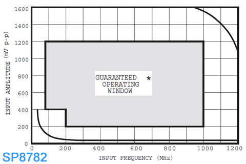
Take, for example, the above chart taken from the datasheet for an SP8782 prescaler. The guaranteed operating window covers the frequency range from 200 MHz to 100 MHz with an input level of 200 mV peak-to-peak, descending to around 50 MHz (according to the datasheet, though the chart makes this look more like 70 MHz) if the input level is increased to 400 mV. However, even lower and higher frequency performance is possible. In the case of lower frequencies, it would appear to operate down to as low as maybe 25 MHz and as high as 1200 MHz if the input levels are suitably adjusted.
Slight aside: The MB501 requires a 2K (or thereabouts) pull-down resistor on its output to function. This isn't optional, it's mandatory. It's easy to forget this and wonder why the circuit isn't working...!
After much research, the MB501L was selected for the Wireless Waffle project. This has a guaranteed minimum operating frequency of 10 MHz, a maximum of 1100 MHz, and over this range will perform correctly with an RF input ranging from -4 to +6 dBm (1 milliWatt give or take). It has a pre-settable division ratio of 64, 65, 128 and 129. What's more one can be bought online for around £1.50 and seems relatively widely available despite originally being of mid 1980s vintage.One other thing to consider when using prescalers is that they often do a rather bad job of isolating their inputs from their outputs (and their power supply rails). This means that the divided signal can easily get into whatever they are connected to, and in particular the RF inputs, causing spurs on the RF signal at multiples of the divider output. Take an example of a 64 MHz oscillator, connected to a device such as the MB501L set to divide by 64. The output frequency of the divider will be 1 MHz, and if care is not taken, this will find its way back into the oscillator meaning that unwanted spurs 1 MHz from the oscillator (i.e. at 63 and 65 MHz) will be produced.
Solutions to this include a buffer between the oscillator and the prescaler, or the introduction of sufficient loss (i.e. through a resistor) between the two to minimise the impact of any lack of isolation in the prescaler. Unless there is an excess of RF power to play with, the best option is to use a buffer. There are a myriad of RF buffer schematics online to choose from. In this application, one of the main criteria is the amount of isolation between input and output as this is the purpose to which the buffer is being put. Another design criteria is for the buffer to produce the right level of output to drive the prescaler at its preferred input levels. Field effect transistor (FET) buffers are particularly good when it comes to input/output isolation, and a very simple buffer can be constructed with the minimum of components. Bipolar transistors (BJT) can also be used, but tend not to have such good isolation. Two such buffer circuits are presented below.
;)
The Junction-FET (JFET) circuit has a very high input impedance (largely set by the value of the 220K resistor from its gate to ground) and good isolation. The input impedance of the BJT circuit will be much lower and isolation poorer, so what, you might ask, is the benefit of the BJT approach. The answer is simple: some companies who manufacture printed circuit boards (PCBs) can also assemble surface mount devices (SMD) on the board at very low prices, and the 2SC3356 shown in the schematic is a device which these manufacturers have in their low-cost stock room, whereas they rarely have JFETs available.
At this point we nearly have all the building blocks necessary to make a fully synthesised transmitter bar a couple - the 'divide by N' block, and the 'phase/frequency comparator'. More, then, to follow soon.
How not to design transmitters and receivers (part 5: phase locked loops)
Thursday 12 August, 2021, 09:39 - Amateur Radio, Broadcasting, Licensed, Pirate/Clandestine, Electronics, Radio Randomness
Posted by Administrator
Parts 1 to 4 of this series have covered generating an RF signal, amplifying it, and providing the whole kit and caboodle with a nice clean power supply. In this part, we consider frequency stabilisation.Posted by Administrator
It is very straightfoward to produce a radio frequency (RF) signal that does not drift from the wanted frequency. Using a quartz crystal oscillator, it is possible to maintain an accuracy of a few parts per million, or a couple of Hz per MHz of output frequency. However, the output from a crystal is so stable that it's just about impossible to move it. If you want to modulate the frequency by more than a few kHz, using a crystal is therefore not feasible. For a wideband FM transmitter, where the required deviation (i.e. the amount by which the frequency changes) is +/- 75 kHz, using a crystal is therefore a non-starter. Instead it is necessary to use a voltage controlled oscillator (VCO) and surround this by some kind of feedback loop which samples the output frequency and corrects it if it has drifted off the wanted frequency. Such a feedback loop is called a phase locked loop or PLL (or indeed a frequency locked loop).
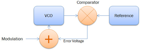
A simple PLL would just compare the frequency being produced by an VCO with some reference, determine the difference between the two, and if the two are different, provide an error voltage to the VCO to bring it back onto frequency. In the block diagram above, the error voltage is added to the modulation voltage as both of them affect the frequency of oscillation. This system would be great, and work a treat, if it was only necessary to operate on one frequency. However, if it is necessary to tune the VCO to different frequencies, some additional jiggery pokery is necessary.
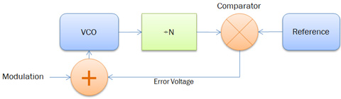
To make a tuneable PLL, an additional stage is added to the loop. The output from the VCO is divided by a number (let's call it 'N') and instead of having a reference frequency the same as the wanted output frequency, a much lower reference frequency is used. For example, if the reference frequency is 100 kHz, and we wanted the VCO to be on 89.6 MHz, we would divide the VCO output by 896 to give 100 kHz, and compare this to the 100 kHz reference. The rest of the circuit then operates as before. If we now change the division ratio to 900 instead of 896, the circuit would now attempt to retune the output to 90.0 MHz (assuming that the VCO was able to tune to that frequency). Thus, by changing the division ratio, we can lock the output frequency to any multiple of the reference frequency that we desire.
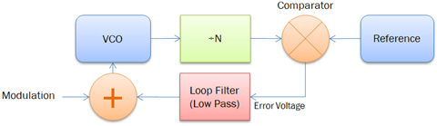
One difficulty of using a PLL in the case where we are trying to modulate the VCO (for example with audio or data) is that the PLL will see any modulation as a frequency error and try and correct it. To circumvent this problem it is normal to filter the error voltage produced by the PLL such that it cannot act upon the VCO at any frequency we are interested in modulating. If we are interested in audio frequencies which may descend as low as 20 Hz, we therefore need to low pass filter the error signal so that it cannot have any effect on modulation frequencies above 20 Hz and thus cannot try and 'correct' the audio being modulated onto the VCO.
This low pass filter is known as the loop filter. In addition to ensuring that the response of the loop is slow enough not to impact any low frequency modulation, it has the dual purpose of removing any of the reference frequency that might be present on the error voltage as the output of the comparator output will often just be a square wave whose mark-space ratio changes depending on the difference between the VCO frequency and the reference. If the required loop response time is slower than 20 Hz, and the reference frequency is 100 kHz this is not a difficult job, however having such a difference between the loop response time and the reference frequency leads to another difficulty: overshoot.
Imagine the situation...
- We switch on the PLL and the output frequency of the VCO is too low. The comparator recognises this and outputs a positive voltage to tell the VCO to increase its frequency. This positive signal is filtered by the loop filter which has the effect of slowing down the response time, and the VCO slowly begins to respond and its frequency rises.
- At some point the VCO output and the reference will now be the same and the comparator will stop producing a positive correction, however the loop filter, being very slow in comparison, has not yet finished acting upon its previous 'increase frequency' instruction and so instead of the PLL settling down, the output frequency continues to rise above the wanted one.
- The comparator now recognises that the frequency is too high and outputs a negative voltage to tell the VCO to reduce its output frequency. This instruction is slowed down by the laggard of the loop filter.
- Eventually the VCO output matches the reference and the comparator stops issuing its correction. But the loop filter has not yet finished the 'reduce frequency' instruction it was given and so the VCO frequency continues to go down.
- The comparator recognises this and outputs a positive voltage to tell the VCO to increase its frequency...
One solution to this is to speed up the loop filter response, but this would then mean that lower modulating frequencies would be corrected by the PLL. Another solution is to reduce the reference frequency so that the loop frequency and the reference frequency are sufficiently close that one does not lag the other too much. This, however, often means that the loop filter will not be able to filter out the comparator output sufficiently, leading to the reference frequency modulating the VCO and causing 'spurs' in the RF output that are separated from the VCO output by the reference frequency.
A common solution to the yo-yo problem is to use a 'lead-lag' filter instead of just a low-pass for the loop filter. A lead-lag filter is a low pass filter whose frequency response is flattened at some point in its frequency range. The advantage of this is that it can provide the filtering necessary to slow down the loop and get rid of the comparator output, whilst providing protection against the yo-yo-ing by having a flatter phase response. This can then be combined with a seperate filter to specifically remove the comparator output and together the two can ensure good performance and a clean VCO output.
How not to design transmitters and receivers (part 4: low drop-out regulators)
Tuesday 3 August, 2021, 07:50 - Amateur Radio, Broadcasting, Licensed, Pirate/Clandestine, Electronics
Posted by Administrator
A quick diversion from RF design to consider, for a short while, the issue of voltage regulation. Voltage Controlled Oscillators (VCOs) need to be supplied with a well regulated and low noise power supply. The power for most equipment is either provided via a mains power supply (which can be full of noise and buzz) or a battery (whose output voltage will decrease over time). Therefore, some manner of regulator is required in order to stabilise the supply and reduce any noise on the supply rail. There are several ways to achieve this:Posted by Administrator
- fixed discrete voltage regulators,
- variable discrete voltage regulators, or
- a purpose designed circuit.
The problem with getting a regulated 10 Volt supply from a 12 Volt input is that the amount of headroom available in which the regulator is able to operate is very limited (just 2 Volts in fact). 10 Volt fixed discrete regulators do exist. The 7810 is one such device, however the datasheet for these regulators clearly states:
The input voltage must remain typically 2.0V above the output voltage even during the low point on the input ripple voltage.
;) So whilst 12 Volts at the input would be just about sufficient to allow the device to do its job, if the input dropped to even 11.9 Volts, there is no guarantee that the regulated output would remain at 10 Volts. The situation is actually more complicated than that, and the necessary voltage drop across the device in order for it to be able to do its job depends on the amount of current it is supplying and the temperature of the device. At low currents and high temperatures the necessary differential between the input and output voltage (the 'dropout' voltage) can be as low as 0.75 Volts, whereas at high current and low temperatures it can reach over 2.2 Volts. Thus, though in principle such a device could provide the 10 Volt regulated supply required, it would be working at the edge of its tolerances and may not provide quite as much regulation as desired.
So whilst 12 Volts at the input would be just about sufficient to allow the device to do its job, if the input dropped to even 11.9 Volts, there is no guarantee that the regulated output would remain at 10 Volts. The situation is actually more complicated than that, and the necessary voltage drop across the device in order for it to be able to do its job depends on the amount of current it is supplying and the temperature of the device. At low currents and high temperatures the necessary differential between the input and output voltage (the 'dropout' voltage) can be as low as 0.75 Volts, whereas at high current and low temperatures it can reach over 2.2 Volts. Thus, though in principle such a device could provide the 10 Volt regulated supply required, it would be working at the edge of its tolerances and may not provide quite as much regulation as desired.Variable voltage discrete regulators (such as the LM317) work on a similar principle to fixed ones, however they are designed to provide a variable output voltage instead of a fixed one. They usually have a reference source of around 1.2 Volts against which another voltage is compared. For example, if you wanted a 12 Volt regulated output, you would use two resistors, one (for the sake of argument) of 900 Ohms, and one of 100 Ohms, connected in series across the output of the power supply. The voltage at the junction of these two resistors when the output voltage was exactly 12 Volts would be 1.2 Volts (12 x 100 / [900+100]). Feed this to the 'comparison' input on the device and it would compare this voltage to its internal 1.2 Volt reference and adjust its output to maintain equilibrium. Thus, by tweaking the value of the resistors, virtually any voltage can be generated. One issue with such a device is that its minimum dropout voltage is generally the same as that of a fixed regulator (as the internal architecture of the devices is much the same) and thus it is also working at the edge of its capabilities with a 2 Volt dropout.
It should be noted that there are a range of Low Dropout (LDO) regulators which can function with much smaller dropout voltages. For example the LM2931 which can operate with a dropout as little as 0.4 Volts. Whilst these may be ideal for this purpose, they aren't readily available in 10 Volt versions and they are not cheap (at least not compared with non-LDO equivalents).
Of course, the Wireless Waffle lockdown radio project could have just decided on using a 9 Volt regulated supply, or an LDO regulator both of which are relatively straightforward, instead of looking to achieve 10 Volts, but what would be the fun in that. Instead the third option of purpose designing a regulator was explored.
The 'bog standard' LDO regulator design which is presented on various forums on the internet is as shown in the circuit below.
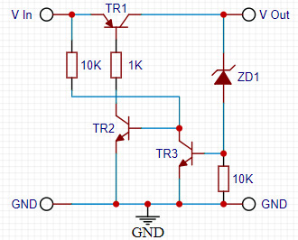
It works on the basis that as the output voltage increases to the point that the Zener diode conducts, the voltage at the base of NPN transistor TR3 increases and as it approaches 0.7 Volts it begins to turn-on. As it does this, it clamps the base voltage of the other NPN transistor, TR2, which turns-off and in the process reduces the current flowing into the base of the PNP transistor TR1 which also turns off reducing the current flowing through it, and thereby lowering the circuit's output voltage (and vice versa for a decrease in output voltage). The output voltage of the regulator is therefore set by the voltage of the Zener diode, ZD1, plus the turn-on voltage of transistor TR3. The reason that this is a low dropout regulator is that the dropout is determined only by the minimum collector-emitter voltage of the PNP transistor, TR1, when it is turned fully on, and this can be as low as 0.2 Volts. The primary issue with this circuit is that its ability to regulate the output voltage is based partially on the turn-on voltage at the base of TR3 and all bipolar transistors are very prone to changes in their turn-on voltage with temperature.
In addition, Zener diodes do not come in every possible Voltage (the nearest you could get to give a 10 Volt output would be to use a 9.1V Zener which together with the turn-on voltage of the transistor of about 0.7 Volts would yield a 9.8 Volt output). Zener diodes are also, like the junction in a bipolar transistor, prone to temperature drift. Thus, what might be a perfect 9.8 Volt output at room temperature might drop to 9.6 Volts at 50C or 10 Volts at -10C - not particularly well regulated.
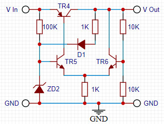
An alternative design (shown above) uses a 'long-tailed pair' (TR5 and TR6) and also uses a Zener diode to provide the voltage reference. Zener diodes of values around 6 Volts have virtually constant temperature characteristics meaning that if used as the voltage reference in a regulator, the output will vary very little as it heats up or cools down. Zener diodes typically need about 5mA of current passing through them to achieve a stable reference voltage and this can be provided from the regulated supply (through D1 and the 1K resistor), ensuring a near constant reference voltage.
The long-tailed pair basically function as an inverter: What one transistor does, the other does the opposite. So if the current in one transistor increases, the current in the other one decreases. The base of NPN transistor TR5 is provide with a fixed voltage reference by the Zener diode, whilst the base of the other senses the output voltage of the circuit via the potential divider made up of the two 10K resistors. The circuit will try and balance the voltage at both bases as follows: If the output voltage decreases, transistor TR6 will draw less current (as its base voltage decreases) and by dint transistor TR5 will draw more current, which forces more current into the base of the PNP transistor, TR4, which will conduct more heavily and increase the output voltage and behold the output voltage is stabilised.
As with a variable regulator, the output voltage can be adjusted by changing the value of the two 10K resistors. As it sits, the output voltage would be exactly 2 times the voltage across the Zener diode. The 100K resistor, by the way, is to provide some initial current for the Zener diode; otherwise, when the circuit is initialised, the Zener voltage and output voltage would both be zero and the circuit would be in equilibrium and nothing else would happen.
This may seem a silly length to go to to produce a low dropout regulator when off-the-shelf ones are available, but oddly, the design using discrete components takes up little more space on a circuit board, performs just as well, and is cheaper. It is also surprisingly good at getting rid of supply hum, buzz, ripple and noise. In addition, if the diode in the circuit (D1) is replaced by a light emitting one (an LED) it will provide an indication that all is well with the regulated output: your off-the-shelf regulator doesn't do that for you now does it?