Wednesday 1 September, 2021, 08:31 - Amateur Radio, Broadcasting, Licensed, Pirate/Clandestine, Electronics
Posted by Administrator
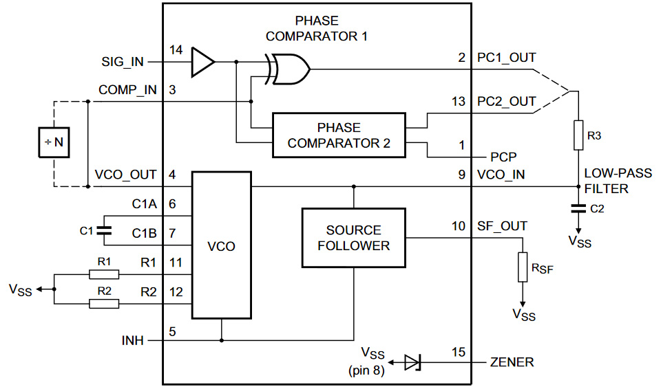
One of the blocks yet to be discussed in the Wireless Waffle lockdown transmitter and receiver project is the phase/frequency comparator. In days of yore (a.k.a. the 1980s), the go-to integrated circuit (IC) for this function was the trusty 4046. This not only contains a couple of different types of phase comparator (the newest versions have three, the older ones just two) it also has a built in voltage controlled oscillator (VCO). The VCO works well up to a few MHz, or even higher depending on the specific type of IC, but is useless at VHF and thankfully can be easily inhibited. As, however, the phase comparator only needs to work at the reference frequency (usually a few kHz), the 4046 will function perfectly well in this role.Posted by Administrator
The 4046 takes the reference input on pin 14 (oddly termed the 'signal in' pin) and the variable frequency input on pin 3 (the 'comparator in'). The two phase comparator outputs are on pins 2 ('comparator I output') and 13 ('comparator II output'). On newer versions a third phase comparator output can be found on pin 15; on the older versions pin 15 has a Zener diode connected to it which is intended to be used to stabilise the power supply when using the VCO but was almost never employed.

The Type I phase comparator is just an XOR gate. This produces a square wave output whose mark-space ratio varies with the difference in phase of the inputs. This can be fed into a loop filter to yield a voltage which varies up or down with the difference in phase. The primary difficulty with this method is that both the reference frequency, and the variable frequency input must be square waves with equal mark-space ratios. For the reference which is usually a square wave divided down from some crystal oscillator, this is usually not a problem, however the signal from the oscillator, following its traversal through the 'divide by N' circuit, is often just a pulse. Many divide by N devices just count a specific number of times, and when that count has been reached output a brief pulse. Additional circuitry is required to turn this into a square wave.
The Type II phase comparator is an altogether more sophisticated device and as well as not caring about the mark-space ratio of the two input signals, produces a positive 'up' or negative 'down' signal at its output instead of just a square wave. If its output is connected to a capacitor (through a suitable current limiting resistor) the voltage across the capacitor will only be given a push up or down if the phase of the input signals is different. If the two are fully in phase, the output of the Type II detector is an open circuit. This massively reduces the amount of the reference frequency that appears at the input to the loop filter, making the whole PLL output cleaner. When modulating the VCO, there will almost inevitably be occasional phase differences so the output will rarely be totally quiet, but this type of detector is generally far easier to work with.
Most modern PLL ICs have a reference oscillator and divider, the divide by N counter, and the phase comparator functions included in them in a single package. Some even have built-in prescalers. Even some older devices integrate several of these functions. The MC145151 which was commonly used in many of the CB radios of the 1980s contains all except the prescaler. The phase detector in this device is akin to the Type II device in the 4046 but has two separate outputs:
- a single pin output mimics the operation of the 4046, with positive and negative pulses and an open circuit when the reference and VCO are in phase, and
- seperate 'up' and 'down' pins which need to be fed into an external combiner/loop filter to generate the voltage to feed the VCO.

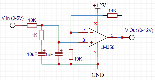
How, then, to get a bigger voltage swing? One method would be to feed the output from the phase comparator into an op-amp with a higher supply voltage, and set up with a gain profile which steps up the 5, 9, 12 or whatever voltage is available from the phase comparator to a higher value. The circuit pictured above will do this. The input from the phase comparator first goes through the previously discussed 'lead-lag' low pass filter. The op-amp is set to have a gain of 2.4, so that a 5 Volt input will give a 12 Volt output. This amplifier, as well as increasing the voltage swing will also, however, amplify any noise at the output of the phase comparator and thus is not ideal.
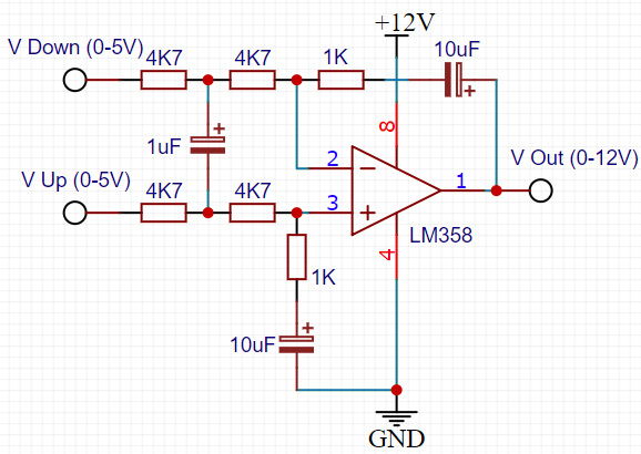
This is where the seperate 'up' and 'down' pin output of devices such as the MC145151 come into their own. Given that there has got to be an external loop filter to use these outputs, this could by default run from a higher supply voltage. Also, as the signals are only nudges up or down, the active loop filter that follows would not further amplify any noise generated by the phase comparator.

The circuit above gives an example of this and has a similar frequency response to the earlier amplifier circuit. It has has a differential input: A positive nudge on the 'V up' input will cause the output voltage to rise and similarly a positive nudge on the 'V down' input will cause the output voltage to fall. When both are silent, the output voltage will hold steady. In this steady state, no noise is being generated or amplified making this kind of approach relatively quiet.
Of course in most cases a 30 Volt supply won't be available (though one could be generated using a simple charge pump but that's for another day), however supplying the amplifier and thus the VCO from even a 12 Volt supply will give an improved frequency range compared to 5 or 9 Volts.
add comment
( 242 views )
| permalink
| 


 ( 2.7 / 788 )


 ( 2.7 / 788 )

