
Tropospheric vs Sporadic-E Propagation Loss
Wednesday 18 August, 2021, 09:35 - Broadcasting, Licensed, Radio Randomness, Spectrum Management
Posted by Administrator
For some time, Wireless Waffle has published an FM DX Logbook. This logbook records any DX (distance) reception of FM broadcast stations that have been received, through whatever means (i.e. home FM tuner, car radio, software radio). Though an interesting exercise in itself, a recent update to the page to show the propagation mode which has been used also included some simple calculations to show the number of metres travelled divided by the number of Watts of transmitter power, and an additional calculation working out what the received signal power would be, assuming free space path loss between the transmitting and receiving location.Posted by Administrator
The use of free space path loss as the propagation model is definitely not applicable for any mode of propagation other than line-of-sight but it proved to be a useful exercise. Based on the frequency and power of the transmitter, and the length of the path, it is possible to determine how strong the received signal would be, if the path was line-of-sight. The results show an interesting trend.
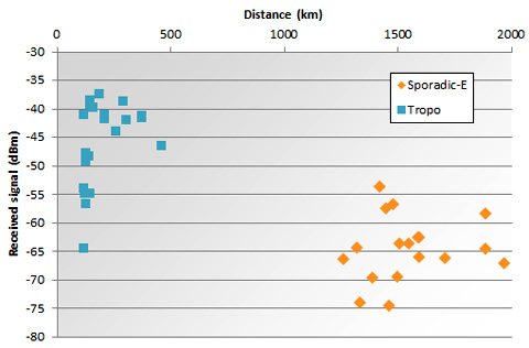
With the exception of a few shorter paths (up to about 150 km), the theoretical signal strengths received from broadcasts received via troposhperic propagation are clustered around -40 dBm (which equates to about 67 dBuV/m). Similarly, the theoretical signal strength of transmissions received via Sporadic-E propagation are clustered around -65 dBm (42 dBuV/m). Note that these are not measured signal strengths, but a calculation of how strong the signals would be if they were being received via a line-of-sight path - which they are not.
A previous Wireless Waffle article identified that around 40dBuV/m is required at a receiver for FM reception. It is almost certainly true, that in the case of both the DX reception via the troposphere, or via Sporadic-E, the actual received signal strength would be similar, as in both cases the signal would need to be strong enough to be successfully received: the necessary signal would be nearer the -65 dBm level than the -40 dBm level. If this is true, then it must also be true that the additional loss caused by a signal travelling via ducts in the troposphere compared to via ionised clouds in the E-layer is around 25 dB, as this is the additional loss which the signal could tolerate and still be received.
This just goes to show how effective Sporadic-E propagation is and why it is (or indeed was) such a problem for VHF television and radio broadcasters during the summer months when it is most prevalent. It also suggests that the path loss via Sporadic-E must be close to the free space value, as if the received signal strength is around 42 dBuV/m based on free space path loss, this is only a couple of dB different to that needed for successful reception and the actual path could not be introducing much in the way of additional attenuation.
add comment
( 188 views )
| permalink
| 

 ( 2.6 / 941 )
( 2.6 / 941 )
How not to design transmitters and receivers (part 5: phase locked loops)
Thursday 12 August, 2021, 09:39 - Amateur Radio, Broadcasting, Licensed, Pirate/Clandestine, Electronics, Radio Randomness
Posted by Administrator
Parts 1 to 4 of this series have covered generating an RF signal, amplifying it, and providing the whole kit and caboodle with a nice clean power supply. In this part, we consider frequency stabilisation.Posted by Administrator
It is very straightfoward to produce a radio frequency (RF) signal that does not drift from the wanted frequency. Using a quartz crystal oscillator, it is possible to maintain an accuracy of a few parts per million, or a couple of Hz per MHz of output frequency. However, the output from a crystal is so stable that it's just about impossible to move it. If you want to modulate the frequency by more than a few kHz, using a crystal is therefore not feasible. For a wideband FM transmitter, where the required deviation (i.e. the amount by which the frequency changes) is +/- 75 kHz, using a crystal is therefore a non-starter. Instead it is necessary to use a voltage controlled oscillator (VCO) and surround this by some kind of feedback loop which samples the output frequency and corrects it if it has drifted off the wanted frequency. Such a feedback loop is called a phase locked loop or PLL (or indeed a frequency locked loop).
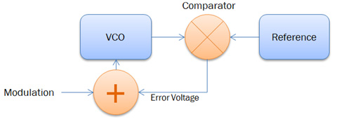
A simple PLL would just compare the frequency being produced by an VCO with some reference, determine the difference between the two, and if the two are different, provide an error voltage to the VCO to bring it back onto frequency. In the block diagram above, the error voltage is added to the modulation voltage as both of them affect the frequency of oscillation. This system would be great, and work a treat, if it was only necessary to operate on one frequency. However, if it is necessary to tune the VCO to different frequencies, some additional jiggery pokery is necessary.
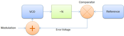
To make a tuneable PLL, an additional stage is added to the loop. The output from the VCO is divided by a number (let's call it 'N') and instead of having a reference frequency the same as the wanted output frequency, a much lower reference frequency is used. For example, if the reference frequency is 100 kHz, and we wanted the VCO to be on 89.6 MHz, we would divide the VCO output by 896 to give 100 kHz, and compare this to the 100 kHz reference. The rest of the circuit then operates as before. If we now change the division ratio to 900 instead of 896, the circuit would now attempt to retune the output to 90.0 MHz (assuming that the VCO was able to tune to that frequency). Thus, by changing the division ratio, we can lock the output frequency to any multiple of the reference frequency that we desire.
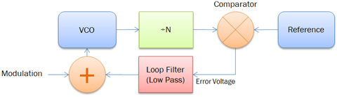
One difficulty of using a PLL in the case where we are trying to modulate the VCO (for example with audio or data) is that the PLL will see any modulation as a frequency error and try and correct it. To circumvent this problem it is normal to filter the error voltage produced by the PLL such that it cannot act upon the VCO at any frequency we are interested in modulating. If we are interested in audio frequencies which may descend as low as 20 Hz, we therefore need to low pass filter the error signal so that it cannot have any effect on modulation frequencies above 20 Hz and thus cannot try and 'correct' the audio being modulated onto the VCO.
This low pass filter is known as the loop filter. In addition to ensuring that the response of the loop is slow enough not to impact any low frequency modulation, it has the dual purpose of removing any of the reference frequency that might be present on the error voltage as the output of the comparator output will often just be a square wave whose mark-space ratio changes depending on the difference between the VCO frequency and the reference. If the required loop response time is slower than 20 Hz, and the reference frequency is 100 kHz this is not a difficult job, however having such a difference between the loop response time and the reference frequency leads to another difficulty: overshoot.
Imagine the situation...
- We switch on the PLL and the output frequency of the VCO is too low. The comparator recognises this and outputs a positive voltage to tell the VCO to increase its frequency. This positive signal is filtered by the loop filter which has the effect of slowing down the response time, and the VCO slowly begins to respond and its frequency rises.
- At some point the VCO output and the reference will now be the same and the comparator will stop producing a positive correction, however the loop filter, being very slow in comparison, has not yet finished acting upon its previous 'increase frequency' instruction and so instead of the PLL settling down, the output frequency continues to rise above the wanted one.
- The comparator now recognises that the frequency is too high and outputs a negative voltage to tell the VCO to reduce its output frequency. This instruction is slowed down by the laggard of the loop filter.
- Eventually the VCO output matches the reference and the comparator stops issuing its correction. But the loop filter has not yet finished the 'reduce frequency' instruction it was given and so the VCO frequency continues to go down.
- The comparator recognises this and outputs a positive voltage to tell the VCO to increase its frequency...
One solution to this is to speed up the loop filter response, but this would then mean that lower modulating frequencies would be corrected by the PLL. Another solution is to reduce the reference frequency so that the loop frequency and the reference frequency are sufficiently close that one does not lag the other too much. This, however, often means that the loop filter will not be able to filter out the comparator output sufficiently, leading to the reference frequency modulating the VCO and causing 'spurs' in the RF output that are separated from the VCO output by the reference frequency.
A common solution to the yo-yo problem is to use a 'lead-lag' filter instead of just a low-pass for the loop filter. A lead-lag filter is a low pass filter whose frequency response is flattened at some point in its frequency range. The advantage of this is that it can provide the filtering necessary to slow down the loop and get rid of the comparator output, whilst providing protection against the yo-yo-ing by having a flatter phase response. This can then be combined with a seperate filter to specifically remove the comparator output and together the two can ensure good performance and a clean VCO output.
How not to design transmitters and receivers (part 4: low drop-out regulators)
Tuesday 3 August, 2021, 07:50 - Amateur Radio, Broadcasting, Licensed, Pirate/Clandestine, Electronics
Posted by Administrator
A quick diversion from RF design to consider, for a short while, the issue of voltage regulation. Voltage Controlled Oscillators (VCOs) need to be supplied with a well regulated and low noise power supply. The power for most equipment is either provided via a mains power supply (which can be full of noise and buzz) or a battery (whose output voltage will decrease over time). Therefore, some manner of regulator is required in order to stabilise the supply and reduce any noise on the supply rail. There are several ways to achieve this:Posted by Administrator
- fixed discrete voltage regulators,
- variable discrete voltage regulators, or
- a purpose designed circuit.
The problem with getting a regulated 10 Volt supply from a 12 Volt input is that the amount of headroom available in which the regulator is able to operate is very limited (just 2 Volts in fact). 10 Volt fixed discrete regulators do exist. The 7810 is one such device, however the datasheet for these regulators clearly states:
The input voltage must remain typically 2.0V above the output voltage even during the low point on the input ripple voltage.
;) So whilst 12 Volts at the input would be just about sufficient to allow the device to do its job, if the input dropped to even 11.9 Volts, there is no guarantee that the regulated output would remain at 10 Volts. The situation is actually more complicated than that, and the necessary voltage drop across the device in order for it to be able to do its job depends on the amount of current it is supplying and the temperature of the device. At low currents and high temperatures the necessary differential between the input and output voltage (the 'dropout' voltage) can be as low as 0.75 Volts, whereas at high current and low temperatures it can reach over 2.2 Volts. Thus, though in principle such a device could provide the 10 Volt regulated supply required, it would be working at the edge of its tolerances and may not provide quite as much regulation as desired.
So whilst 12 Volts at the input would be just about sufficient to allow the device to do its job, if the input dropped to even 11.9 Volts, there is no guarantee that the regulated output would remain at 10 Volts. The situation is actually more complicated than that, and the necessary voltage drop across the device in order for it to be able to do its job depends on the amount of current it is supplying and the temperature of the device. At low currents and high temperatures the necessary differential between the input and output voltage (the 'dropout' voltage) can be as low as 0.75 Volts, whereas at high current and low temperatures it can reach over 2.2 Volts. Thus, though in principle such a device could provide the 10 Volt regulated supply required, it would be working at the edge of its tolerances and may not provide quite as much regulation as desired.Variable voltage discrete regulators (such as the LM317) work on a similar principle to fixed ones, however they are designed to provide a variable output voltage instead of a fixed one. They usually have a reference source of around 1.2 Volts against which another voltage is compared. For example, if you wanted a 12 Volt regulated output, you would use two resistors, one (for the sake of argument) of 900 Ohms, and one of 100 Ohms, connected in series across the output of the power supply. The voltage at the junction of these two resistors when the output voltage was exactly 12 Volts would be 1.2 Volts (12 x 100 / [900+100]). Feed this to the 'comparison' input on the device and it would compare this voltage to its internal 1.2 Volt reference and adjust its output to maintain equilibrium. Thus, by tweaking the value of the resistors, virtually any voltage can be generated. One issue with such a device is that its minimum dropout voltage is generally the same as that of a fixed regulator (as the internal architecture of the devices is much the same) and thus it is also working at the edge of its capabilities with a 2 Volt dropout.
It should be noted that there are a range of Low Dropout (LDO) regulators which can function with much smaller dropout voltages. For example the LM2931 which can operate with a dropout as little as 0.4 Volts. Whilst these may be ideal for this purpose, they aren't readily available in 10 Volt versions and they are not cheap (at least not compared with non-LDO equivalents).
Of course, the Wireless Waffle lockdown radio project could have just decided on using a 9 Volt regulated supply, or an LDO regulator both of which are relatively straightforward, instead of looking to achieve 10 Volts, but what would be the fun in that. Instead the third option of purpose designing a regulator was explored.
The 'bog standard' LDO regulator design which is presented on various forums on the internet is as shown in the circuit below.
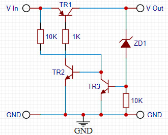
It works on the basis that as the output voltage increases to the point that the Zener diode conducts, the voltage at the base of NPN transistor TR3 increases and as it approaches 0.7 Volts it begins to turn-on. As it does this, it clamps the base voltage of the other NPN transistor, TR2, which turns-off and in the process reduces the current flowing into the base of the PNP transistor TR1 which also turns off reducing the current flowing through it, and thereby lowering the circuit's output voltage (and vice versa for a decrease in output voltage). The output voltage of the regulator is therefore set by the voltage of the Zener diode, ZD1, plus the turn-on voltage of transistor TR3. The reason that this is a low dropout regulator is that the dropout is determined only by the minimum collector-emitter voltage of the PNP transistor, TR1, when it is turned fully on, and this can be as low as 0.2 Volts. The primary issue with this circuit is that its ability to regulate the output voltage is based partially on the turn-on voltage at the base of TR3 and all bipolar transistors are very prone to changes in their turn-on voltage with temperature.
In addition, Zener diodes do not come in every possible Voltage (the nearest you could get to give a 10 Volt output would be to use a 9.1V Zener which together with the turn-on voltage of the transistor of about 0.7 Volts would yield a 9.8 Volt output). Zener diodes are also, like the junction in a bipolar transistor, prone to temperature drift. Thus, what might be a perfect 9.8 Volt output at room temperature might drop to 9.6 Volts at 50C or 10 Volts at -10C - not particularly well regulated.
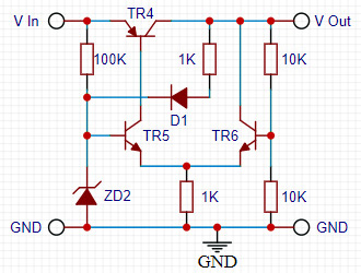
An alternative design (shown above) uses a 'long-tailed pair' (TR5 and TR6) and also uses a Zener diode to provide the voltage reference. Zener diodes of values around 6 Volts have virtually constant temperature characteristics meaning that if used as the voltage reference in a regulator, the output will vary very little as it heats up or cools down. Zener diodes typically need about 5mA of current passing through them to achieve a stable reference voltage and this can be provided from the regulated supply (through D1 and the 1K resistor), ensuring a near constant reference voltage.
The long-tailed pair basically function as an inverter: What one transistor does, the other does the opposite. So if the current in one transistor increases, the current in the other one decreases. The base of NPN transistor TR5 is provide with a fixed voltage reference by the Zener diode, whilst the base of the other senses the output voltage of the circuit via the potential divider made up of the two 10K resistors. The circuit will try and balance the voltage at both bases as follows: If the output voltage decreases, transistor TR6 will draw less current (as its base voltage decreases) and by dint transistor TR5 will draw more current, which forces more current into the base of the PNP transistor, TR4, which will conduct more heavily and increase the output voltage and behold the output voltage is stabilised.
As with a variable regulator, the output voltage can be adjusted by changing the value of the two 10K resistors. As it sits, the output voltage would be exactly 2 times the voltage across the Zener diode. The 100K resistor, by the way, is to provide some initial current for the Zener diode; otherwise, when the circuit is initialised, the Zener voltage and output voltage would both be zero and the circuit would be in equilibrium and nothing else would happen.
This may seem a silly length to go to to produce a low dropout regulator when off-the-shelf ones are available, but oddly, the design using discrete components takes up little more space on a circuit board, performs just as well, and is cheaper. It is also surprisingly good at getting rid of supply hum, buzz, ripple and noise. In addition, if the diode in the circuit (D1) is replaced by a light emitting one (an LED) it will provide an indication that all is well with the regulated output: your off-the-shelf regulator doesn't do that for you now does it?
How not to design transmitters and receivers (part 3: RF matching)
Sunday 25 July, 2021, 20:31 - Amateur Radio, Broadcasting, Licensed, Pirate/Clandestine, Electronics, Radio Randomness
Posted by Administrator
Part 1 of this series investigated an oscillator to generate an RF signal, and Part 2 looked at output devices which can produce 1 Watt. In order to connect one to the other, an intermediate amplifier is usually required. This provides additional gain to make sure that the output device has enough drive and buffers the oscillator from any changes in the output load. There are plenty of transistors (including surface mount) that are capable of providing the necessary amplification, so this is easy. For the Wireless Waffle lockdown project, an MPSH10 transistor was used. This is capable of a around 150mW of output, has plenty of gain at VHF frequencies, is cheap, and is readily available. A surface mount equivalent (the MMBTH10) is also available if needed. Posted by Administrator
Easy right? Drive the input of the transistor from the oscillator, and connect it's output to the RF power device. Not quite so. The main difficulty is that the input impedance of the RF output transistor is very low, whereas the output impedance of the preceding amplifier is relatively high.
The output impedance of the intermediate amplifier can be calculated based on the output power it is required to deliver. The equation is as follows:
Rout = V2/2Po
where:
- Rout is the optimum load resistance of the amplifier.
- V is the Voltage swing at the output of the amplifier. This is generally the power supply voltage minus the voltage drop across the transistor when it is in operation.
- Po is the required output power in Watts.
How, then, to match a 300 Ohm output impedance to a 3 Ohm input impedance? Inter-stage impedance matching can be achieved either via transformers (which can offer broad bandwidth solutions), or by various arrangements of capacitors and inductors (which tend to need to be tuned around specific frequencies). The ratio of turns in a transformer is the square root of the ratio of the impedances, so in this case, a transformer would have to have a turns ratio of roughly 10:1. Such large impedance transformation ratios are difficult to achieve with transformers (for various as yet undiscussed reasons) and so an alternative approach is needed.
Impedance matching using basic networks made of inductors (L's) and capacitors (C's) can easily be done, however a simple two or three component network capable of converting from 500 to 3 Ohms would require a circuit with a minimum 'Q' factor of around 11. The Q factor determines the bandwidth of the network and roughly speaking if you divide the operating frequency by the Q, you get the half-power (3dB) bandwidth of the network. At 100 MHz for example, such a network would have a bandwidth of around 9 MHz, or put another way plus or minus 4.5 MHz from the centre frequency. This would work, but would clearly require re-tuning if the transmitter wanted to operate at different frequencies within the FM band, and as has been previously stated, any part that needs to be adjusted is subject to many potential failure modes.
So how's about a more complicated LC matching network? Calculating the necessary component values for LC matching networks with up to 4 components can be done relatively easily, and to make matters even more straightforward there is an online tool which will do it for you. The Impedance Matching Network Designer will do all the difficult sums. Just enter the input and output impedance you are trying to match and the web-site will do the necessary maths.
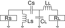 Entering 3 ohms and 300 ohms into the values for the load and source resistance respectively, results in a range of possible network topograhpies (fancy words which mean the relative positions of the L's and the C's). Some of these are more useful than others, and the one selected was the L-C-C-L network as depicted on the right. The values given by the calculator are as follows:
LS = 159 nH
CS = 17.6 pF
CL = 159 pF
LL = 14.3 nH
The advantage of this arrangement is that LS can be made the inductor which sits between the collector of the transistor and the power supply, providing it's power source and thus slightly reducing overall component count. Simulating this network using the excellent Micro-Cap tool (which is amazingly now free) from the appropriately named Spectrum Software and driving it directly from the collector of the MPSH10 showed a rather lumpy frequency reponse (shown below in blue - click for a larger version).;)
After some tweaking it was found that changing CS to 15 pF and CL to 180 pF, and adjusting LS and LL accordingly gave a better and less lumpy match between the two stages, and at the same time had sufficient bandwidth that no re-tuning of the network is needed across the frequency range 88 to 108 MHz (the red curve on the graph). This, incidentally, does not mean that changing the values can not give a better result. A 'broadband' matching network will almost always represent a compromise on the overall matching efficiency and playing around with the values can give additional gain on a particular frequency at the expense of a reduction in gain on a different frequency. However, as long as the output device and its driver have sufficient oomph to produce the required output across the whole frequency range, there is little to benefit from the extra gain. Of course, in real life, with actual (and not simulated) components the values may need further tweaking.