
How not to design transmitters and receivers: part 17 (PCB and kit)
Monday 7 March, 2022, 09:49 - Broadcasting, Licensed, Pirate/Clandestine, Electronics
Posted by Administrator
There seems to have been a lot of interest in the Wireless Waffle series entitled 'How Not to Design Transmitters and Receivers'. One or two (or, indeed, a few more) people have asked about a printed circuit board (PCB) layout and even whether it might be possible to put a kit of parts and set of instructions together for experimenters who wanted to try and build a 1 Watt FM transmitter/exciter for themselves. In that vein, a PCB has been designed for a simple synthesised PLL transmitter which has the following characteristics. It:
Posted by Administrator
- Uses a half-frequency oscillator, to get round the feedback problems that an at-frequency oscillator can suffer from in RF hot environments
- Is built from the minimum sub-set of components, to keep the cost of getting all the parts together as low as possible
- Doesn't use lots of obsolete, expensive or difficult-to-get-hold-of parts
- Can accommodate different output transistors (such as the 2N4427, MRF237 and similar)
- Can use a range of transistors for most of the parts (such as the BF199, MPSH10 and similar)
- Will produce around 1 Watt across the band with as little fiddling as possible (or more depending on the output transistor)
- Has an output that is legally clean enough to either be connected directly to an antenna, or amplified to high power (nothing over 60dB below the carrier)
- Keeps the digital and analogue parts of the circuit as seperate as possible to minimise digital noise on the modulation
- Doesn't require any micro-controllers and thus does not require any software to be written/blown
- Has out-of-lock power-down to stop transmissions on unwanted frequencies whilst the phase lock loop is settling down
- Is straightforward to set onto the desired frequency
- Can be easily tested and maintained (to the extent that it could be built in stages, testing each along the way)
- Has a flat modulation frequency response from around 3 Hz to at least 100 kHz, providing superlative audio
- Does not need any tuning (other than setting the VCO frequency)
- Can have its output quickly disabled (i.e. for connection to a high SWR detector)
- With some component changes, can be made to work on Band-I too (the final design will work down to about 52 MHz)
There are no surface-mount parts on the PCBs, making it easy to assemble even for the relatively cack-handed, and the ICs can be socketted for those not confident enough to solder the chips directly to the board. The only complexity is that there are a number of coils to be manually wound, including one on a small toroid.
The circuit diagram is below and those who have followed the series will recognise the various elements which go together to make up the overall design.
;)
Three options are available for anyone who wishes to have a go a building this design:
- PBC's for this project are available on their own for those who wish to assemble the various components required themselves, or who have a large junk-box full of suitable components. This is £4.99 plus postage.
- In addition, a minimalist kit is available which contains the PCB, as well as the ICs, transistors and the toroid and wire for winding the coils as these are the parts least likely to be in a typical junk box. This is £24.99 plus postage.
- Finally, a full kit of parts is available including the PCB, semi-conductors, toroids and all the resistors, capacitors and diodes needed to complete the project. This is £34.99 plus postage.
To get hold of your FM 3.05K kit, please leave a postcard with your name and address, together with £10,000 in unmarked £20 notes in a rucksack in a dustbin of your choice at Piccadilly railway station in Manchester at 23:15 any sunny Tuesday night in March.
Alternatively, fill in the contact form, stating which version of the kit you wish to purchase, and where it needs posting to, and we'll get back to you with a final price (including the postage) and how to pay (this will be via PayPal).
add comment
( 607 views )
| permalink
| 

 ( 2.9 / 1110 )
( 2.9 / 1110 )
The mystery of TOP Radio, Ypres
The Wireless Waffle FM DX Logbook has been updated to automatically calculate the theoretical signal levels, following a previous article that discussed whether any conclusions could be drawn about whether sporadic-E and tropospheric propagation produced different path losses. As a result of the update, the logbook page now draws the chart which shows the theoretical signal level produced by different transmitters.
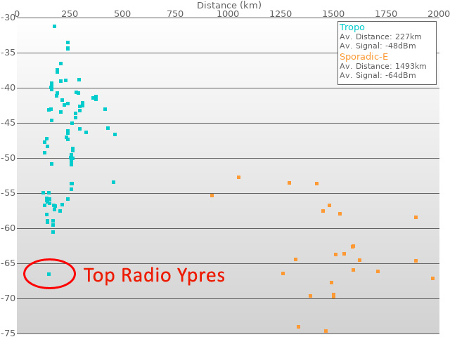
With all of the logs now included in the calculations, the difference in propagation loss is smaller than that which was original posited, however it shows that the theoretical average signal from a radio station received via tropospheric propagation is around -48 dBm, whereas one received via sporadic-E propagation is around -64 dBm, a still not insubstantial 16 dB difference, suggesting that tropo propagation is more lossy than sporadic-E (as the received signal strengths are very similar).
What also stands out from the chart is the single outlying value in the blue, tropospheric values. One dot exists at around -66 dBm which is over 6dB lower than for any other station. This dot represents the theoretical signal from TOP Radio, from its 105.7 MHz FM transmitter in Ypres (Belgium), which has a supposed transmitter power (according to FM Scan, and the ITU GE06 database) of 100 Watts. This station has been logged on more than one occasion so it is not just a one-off freak of reception that it appears on the chart.
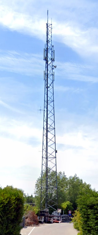
Image capture: Jun 2021 Ⓒ 2022 GoogleThere are several possible explanations for the anomoly:
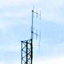 It is not easy to see from the picture above and to the right, however using Google Street View it is possible to get a side look at the mast. Mounted on top are two, three element, vertically polarised antennas pointing roughly north west (as they would need to, to provide coverage in Ypres from the transmitter site). Again, it is difficult to tell, but a working assumption might be that these are the antennas used for TOP Radio, not least as they are the only ones that would be near the 30 metre height that the records suggest that they should be mounted at. It may be that the '100 Watt' power restriction has been interpreted as 100 Watts to the antenna, rather than 100 Watts e.i.r.p.
If we presume that:
If the e.i.r.p. of TOP Radio is closer to 800 Watts than 100 Watts, this would account for the anomoly in the received signal chart, and so the mystery is, at least partially, solved. Let's just hope that the authorities in Belgium responsible for regulating FM radio transmitters don't read this!
;)
With all of the logs now included in the calculations, the difference in propagation loss is smaller than that which was original posited, however it shows that the theoretical average signal from a radio station received via tropospheric propagation is around -48 dBm, whereas one received via sporadic-E propagation is around -64 dBm, a still not insubstantial 16 dB difference, suggesting that tropo propagation is more lossy than sporadic-E (as the received signal strengths are very similar).
What also stands out from the chart is the single outlying value in the blue, tropospheric values. One dot exists at around -66 dBm which is over 6dB lower than for any other station. This dot represents the theoretical signal from TOP Radio, from its 105.7 MHz FM transmitter in Ypres (Belgium), which has a supposed transmitter power (according to FM Scan, and the ITU GE06 database) of 100 Watts. This station has been logged on more than one occasion so it is not just a one-off freak of reception that it appears on the chart.
;)
Image capture: Jun 2021 Ⓒ 2022 Google
- The transmitter site is at a particularly elevated location, improving the coverage of the station. However, according to various sources it is only 40 to 43 metres above sea level, which isn't particularly high.
- The antenna is mounted very high above the ground. Again, according to FM Scan, it is only 30 metres above ground level, which isn't an outstanding lofty height, as the picture on the right of the transmitter site shows.
- The transmitter power is not the stated 100 Watts. For the 'dot' on the chart to be better grouped with the other stations received, the transmitter power would have to be at least 6dB higher, i.e. 400 Watts, or even higher.
- There is some freak propagation path from Ypres to the UK that occurs on regular occasions, and to different UK receive locations, which gives TOP Radio an advantage over other stations in its neighbourhood.
- There is an alien spacecraft hovering mid way between the UK and Belgium which is reflecting or relaying the signal with surprising effectiveness.
It is not easy to see from the picture above and to the right, however using Google Street View it is possible to get a side look at the mast. Mounted on top are two, three element, vertically polarised antennas pointing roughly north west (as they would need to, to provide coverage in Ypres from the transmitter site). Again, it is difficult to tell, but a working assumption might be that these are the antennas used for TOP Radio, not least as they are the only ones that would be near the 30 metre height that the records suggest that they should be mounted at. It may be that the '100 Watt' power restriction has been interpreted as 100 Watts to the antenna, rather than 100 Watts e.i.r.p.If we presume that:
- 100 Watts is being fed up the coax to the antennas; and
- the gain of each 3 element antenna is 6 dB relative to a dipole (a reasonable figure); and
- the additional gain from stacking 2 dipoles is 3 dB;
If the e.i.r.p. of TOP Radio is closer to 800 Watts than 100 Watts, this would account for the anomoly in the received signal chart, and so the mystery is, at least partially, solved. Let's just hope that the authorities in Belgium responsible for regulating FM radio transmitters don't read this!
How not to design transmitters and receivers: part 16 (FM demodulator)
Thursday 9 December, 2021, 15:57 - Amateur Radio, Broadcasting, Licensed, Pirate/Clandestine, Electronics
Posted by Administrator
In the grand tradition of Wireless Waffle, instead of starting at the beginning of the receiver design, we shall tackle the end, the de-modulator, first. There are a number of ICs that will de-modulate wideband FM signals including modern chips which can act as a complete receiver chain. Notwithstanding these, however, the age old (actually 40 year old) CA3089 and CA3189 (a.k.a. HA1137) are capable IC's which have both technical and economic advantages:
Posted by Administrator
- They are easy to work with, requiring few external parts.
- They can be modified to work with different channel bandwidths and deviations.
- They yield very decent audio signal to noise ratios for strong signals (in excess of 70 dB).
- They have decent AM rejection (i.e. the ability to ignore signal fluctuations).
- They have relatively low audio distortion (around 0.5% THD in a standard configuration).
- They are easy to get hold of.
- They are cheap.
Intermediate frequency (IF) filters typically used in wideband FM receivers are usually based on ceramic filters which almost always have an impedance around 330 Ohms. This means that the input impedance of the de-modulator must be 330 Ohms to match the filter properly and ensure that the performance and frequency response of the filter are correctly achieved. The input impedance of the CA3089/3189 itself is not specified in the datasheet but is generally regarded as being 'high' (i.e. a few kilo Ohms). As such, to match the 330 Ohm impedance of the filter it is simply a matter of placing a 330 Ohm resistor across the input of the chip, as the effect of the parallel input impedance of the chip would be negilgable.
The only other design decision is what channel bandwidth and deviation are to be used. For an 'off-the-shelf' wideband FM transmission, the occupied bandwidth is a smidge over 250 kHz and the deviation is 75 kHz, so this is what the circuit will be designed for. The way in which the IC demodulates the FM signal is to apply the incoming signal to a tuned-circuit via a relatively high impedance inductor. The overall frequency and phase reponse of the circuit is shown in the figure below with frequency response in blue, and phase response in red.
;)
As can be seen, there is a rapid change of phase as the frequency sweeps past 10.7 MHz, and it is this change which the IC uses to demodulate the audio of the FM transmission. The more linear the phase response, the less distorted the recovered modulation is. Ideally the phase change should be a straight line (a straight green line has been drawn on the graph for comparison). For low distortion demodulation of an FM signal at 10.7 MHz, the phase change line should be as flat as possible between approximately 10.575 and 10.825 MHz.
Changing the required bandwidth or deviation response of the receiver entails modifying these 'phase discriminator' components to alter their phase response. The circuit of a simple CA3089/3189 based FM demodulator is shown below. Note that there are a couple of small component differences between the CA3089 and CA3189 circuits.
;)
Some of the pins are shown as being not connected. These relate to a 'mute' circuit which switches off the audio output of the device if there is no incoming signal (often called 'squelch'). This is very useful if being used for a hi-fi receiver as it means that when tuned to the emptiness between stations on the FM dial, the receiver goes quiet rather than emitting a loud hissing noise. It does, however, make it more difficult to eke out weak signals as if they are too weak, they will be muted and therefore they have been left unconnected.
How not to design transmitters and receivers: part 15 (receiver gain distribution)
Monday 22 November, 2021, 20:32 - Amateur Radio, Broadcasting, Licensed, Pirate/Clandestine, Electronics
Posted by Administrator
Before addressing each of the building blocks required for a receiver, it is first important to consider the necessary gain distribution of the circuit and the various elements that make it up, that is to say the amount by which the signal needs to be amplified before it reaches the de-modulator. Set the gain too low and the receiver will lack sensitivity. Set the gain too high and not only is there a chance that it may self-oscillate due to the excessive gain, but the de-modulator may be driven with unnecessarily high signals which impede its performance.Posted by Administrator
The age old CA3089 (and the later CA3189) is still a good building block for a wide-band FM receiver as it has acceptably good noise performance, is easy to use, and has all the features needed (such as a signal strength indicator output) for most applications. The datasheet for the CA3089 shows that it begins to develop an audio output when the input to it reaches 12 microVolts. At this point it is 3dB down (half power) and rises to maximum output very quickly.
Now for some maths:
- Let us assume that the bandwidth of the receiver is 250 kHz (this is set by the IF filters) which is about correct for a wideband FM receiver.
- The amount of thermal (background) noise generated in 250 kHz of bandwidth into a 50 Ohm load is 0.45 microVolts - this is the amount of noise that would be naturally present at the input to the receiver based on the kTB formula where 'k' is Boltzmann's constant, T is the temperature of the receiver in degrees Kelvin (usually regarded as 290K) and B is the bandwidth in Hz.
- Note that man-made noise and other factors will increase this level at the antenna and thus the input level of the receiver will be somewhat higher. In addition, unless the receiver is noiseless (which is impossible) it will, itself, generate additional noise above and beyond this level, the amount of this is known as the noise figure or noise factor. However, let's use the thermal noise as the theoretical minimum input.
- The necessary voltage gain of the receiver from its RF input to the input of the CA3089 therefore needs to be a factor of 26.6 (12/0.45), or a power gain of 28 dB.
- The input band-pass filter may have a gain (actually a loss) of -2 dB (lower loss filters can be generated, but we shall be cautious in this regard).
- Mixers have not yet been discussed, however the NE602 which will be introduced later and used to perform the job of the mixer has a gain of +17 dB.
- This means that the IF stage which usually comprises a filter and an amplifier needs to have a gain of +13 dB to make the overall gain correct.
- A typical ceramic 10.7 MHz IF filter will have a loss of around -6 dB, meaning that to correct the overall gain, the IF amplifier needs approximately +19 dB of gain.
;)
This arrangment of gain means that the de-modulator will see the background (thermal) noise as strong enough to begin to de-modulate audio. Any actual received signal will therefore be above this level and will be strong enough for the device to work correctly.