Thursday 16 September, 2021, 16:18 - Amateur Radio, Broadcasting, Licensed, Pirate/Clandestine, Electronics
In an earlier 'How not to design transmitters and receivers' it was blithely stated that the reference oscillator part of a phase locked loop (PLL) was a relatively trivial undertaking. And... it is. All that needs to be decided is what the reference frequency is going to be.Throughout these series of articles, a reference frequency of 100 kHz has been used in order to illustrate how a variable frequency PLL operates. However, this would require that the output frequency is fed directly into the 'divide by N' block, and as has also been discussed, these devices do not usually operate at frequencies as high as 100 MHz, indeed many of the purpose-designed divide by N chips (such as the TC9122P) will only cope with input frequencies as high as 10 to 15 MHz. In addition, as was discussed in part 5, the lower the reference frequency, the less the PLL will see modulation as a frequency error and try and correct it. A reference frequency of 100 kHz is therefore both difficult to work with (due to the divide by N frequency limitations) and too high (due to the PLL trying to correct modulation).
How high should the reference frequency be then? In many PLL designs for FM transmitters, this is often set to be in the order of 10 kHz, though some designs are nearer 1 kHz. For the Wireless Waffle lockdown project, it was decided to use an even lower frequency, so that the low frequency audio response of the PLL could be as flat as possible.
To define the exact frequency, the amount by which the prescaler initially divides down the output frequency must be factored in. The previously discussed MB501L can be set to divide by 64 or 128. If either of these were immediately followed by a divide by N, which could count in steps of 1 and with each step being 100 kHz, then the maximum reference frequency would be either 1.5625 kHz (100 kHz / 64) or 781.25 Hz (100 kHz / 128). The reference frequency could be lower than this if, for example, the divide by N used a higher division ratio (for example, counting in steps of 2). To allow for 25 kHz steps, which are used in some other audio applications such as studio-to-transmitter links, a reference frequency of 390.625 Hz was chosen (i.e. 25 kHz / 64). Note that this means that for each 100 kHz step, the divide by N counter has to be incremented by 4, not 1.
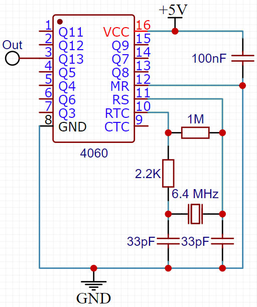
 The simplest way of generating a reference frequency is to use the tried and tested 4060 IC as shown in the circuit on the right. The 4060 has a built in oscillator (which can be used with quartz crystals such as in this application, or as just with resistors and capacitors) as well as having a binary counter that can easily produce outputs divided by multiples of 2. Even the standard CMOS version of this chip will oscillate at frequencies up to around 8 MHz with a 5 Volt power supply and higher still if the supply voltage is increased.
A crystal with a frequency of 6.4 MHz is easy to source (being a not-uncommon clock frequency) and needs to be divided by 16384 (or 214) to produce an output at the required reference at 390.625 Hz. The 4060 has an output which divides by 214 on pin 3 so a simple crystal oscillator and divider circuit can be made from this chip alone.
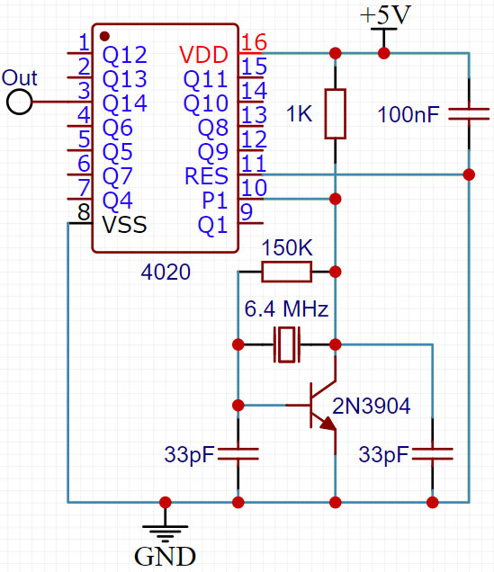
 Other CMOS divider chips (such as the 4020, 4024 or 4040) can also be used for dividing down a fixed frequency oscillator but need a stand-alone crystal oscillator to drive them. An example of this arrangement is shown on the left.
Note that the value of resistors around the transistor used as the oscillator are somewhat critical. The exact current flowing through the transistor is not that critical (anywhere in the region of 2 to 5 milliAmps should be OK) however the transistor needs to be biassed such that when it is not oscillating, the collector voltage is close to half the supply voltage. This will mean that when oscillating the output swings equally above and below half the supply voltage, which the CMOS counter, whose input thresholds are similarly symmetrical, will count properly. In the case of the transistor being biassed such that the output when not oscillating sits at say, 3/4 of the supply voltage, it is possible that the peak-to-peak output swing may be reduced and may not be sufficient to drive the CMOS chip. These resistor values will be different depending on the exact transistor used (actually the specific DC current gain, β, or hFE of the transistor). As with many electronic design problems these days, there's an online tool to help calculate the necessary resistor values..
 And so, the end is near, and that final curtain is nearly ready to be opened to a blaze of audience applause. In the next article in this series, everything learnt so far will be soldered together into a single circuit diagram (or schematic, whichever is your preference). And then it will be time to start to think about receivers, and their associated building blocks. Some say that radio frequency (RF) design is a bit of a black art, insofar as there are so many hurdles which can trip you up along the way (if that isn't a badly mixed metaphor). For transmitters, the biggest problems come from unwanted harmonics and crazy spurious oscillations. In receivers there are these things to deal with, but also the need to have a nice clean and distortion path from the input to the output so that the wanted signal can be received, and any unwanted signals can be rejected. Nobody said it was easy.